AC701N_PMU_介绍
AC701N_PMU_介绍
AC701N_PMU_介绍 用户手册
Rev 1.1——2022年5月30 日
This translated version is for reference only, and the English version shall prevail incase ofany discrepancy between the translated and English versions.
版权所有 2022杰理科技有限公司未经许可,禁止转载
目录
Chapter 1 简介............................................................................................................................................... 4
- 1说明..................................................................................................................................................... 4
1.2 名词解释............................................................................................................................................ 4
1.3 配置及接口路径................................................................................................................................ 4
1.4 特征.................................................................................................................................................... 5
Chapter 2 寄存器........................................................................................................................................... 6 - 1说明..................................................................................................................................................... 6
2.2 p33_ i。 .................................................................................................................................................. 6
Chapter 3 参数配置..................................................................................................................................... 12
3.1 电源参数........................................................................................................................................... 12 - 2边沿唤醒........................................................................................................................................... 13
Chapter 4 唤醒............................................................................................................................................. 15 - 1简介................................................................................................................................................... 15
4.2 接口使用.......................................................................................................................................... 15
Chapter 5 复位............................................................................................................................................. 18 - 1简介................................................................................................................................................... 18
5.2 接口使用.......................................................................................................................................... 18
Chapter 6 校准............................................................................................................................................. 20
Chapter 7 低功耗......................................................................................................................................... 21
7.1 简介.................................................................................................................................................. 21
7.2 i。配置............................................................................................................................................... 21
6.3 低功耗检查配置.............................................................................................................................. 24
Chapter 8 客户常见问题反馈解答............................................................................................................... 27
Q1: ........................................................................................................................................................ 27
Q2: ........................................................................................................................................................ 27
AC701N All information provided in this document is subject to legal disclaimers © JL.V. 2019. All rights reserved.
User manual Rev1. 1——2022/5/30 2of27
修改日志
| 版本 | 日期 | 描述 |
|---|---|---|
| 1.0 | 2022 / 5 / 10 | AC701N初始化版本 |
| 1.1 | 2022 / 5 / 30 | 更新边沿唤醒接口、添加低功耗时间参数说明 |
AC701N All information provided in this document is subject to legal disclaimers © JL.V. 2019. All rights reserved.
User manual Rev1. 1——2022/5/30 3of27
Chapter 1 简介
1. 1说明
该文档主要描述AC701N_SDK PMU 的使用方法及开发中注意的一些问题,调试方法,具体使用方法主要包括包括板级配置、相关接口、PMU CPU等,为用户进行二次开发提供参考(由于电源配置每个方案会有细微不同,请开发人员仔细查看配置方法及接口使用!!!)。
AC701N 内置pmu, 由 P11与P33组成,其中 P11为32位CPU。 支持包含电源、 唤醒、 复位、 Sensor Hub等功能,支持低功耗模式powerdown、 poweroff、 softoff。
1.2 名词解释
运行状态:系统在工作,没有进入低功耗。
低功耗:包括powerdown、 poweroff、 softoff
软关机:softoff,系统掉电睡眠/sleep:powerdown/poweroff,根据应用流程选择对应模式, 由系统调度进入 DCVDD:即VDC12、 VDC13,低压模块供电
IOVDD:即VDDIO, IO 电源端,有强与弱区分,系统进入低功耗为弱驱动
MIOVDD:即VDDIOM,运行状态下的vddio 电源端
WIOVDD:即VDDIOW,低功耗下的vddio 电源端
唤醒:将CPU从低功耗状态下唤醒,并可以产生对应中断
1.3 配置及接口路径
电源参数:板级文件board_xxx_cfg.c, power_param
唤醒参数:板级文件board_xxx_cfg.c, wk_param
所有接口:include/driver/cpu/$(CPU)/asm/ power_interface. h
AC701N All information provided in this document is subject to legal disclaimers © JL.V. 2019. All rights reserved.
User manual Rev1. 1——2022/5/30 4of27
1.4 特征
以下电源特性参考Datasheet,需要注意低功耗模式、运行状态下的 IOVDD 的驱动力。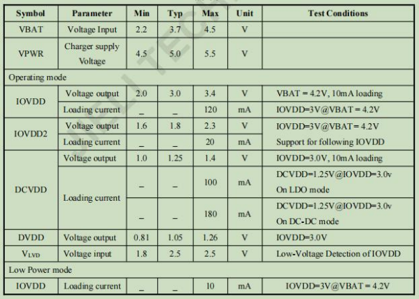 AC701N All information provided in this document is subject to legal disclaimers © JL.V. 2019. All rights reserved.
User manual Rev1. 1——2022/5/30 5of27
Chapter 2 寄存器
2. 1说明
本章节介绍一些pmu使用的寄存器,方便用户了解硬件及快速使用。
2.2 p 33_io
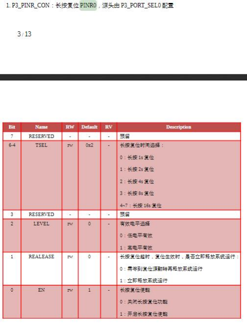
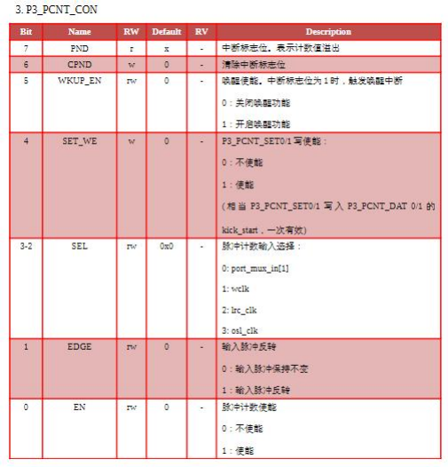
1、 p33系统的io主要功能有:长按复位、边沿唤醒、脉冲计数。
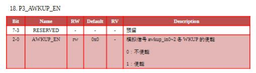
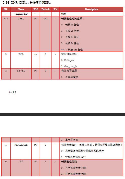
2、 gpio数字输入io选通如下,该输入信号可以作为长按复位(数字)、 边沿唤醒(数字)、 脉冲计数的输入源,其中通道0为长按复位与边沿唤醒复用,通道1为脉冲计数与边沿唤醒复用。 唤醒参数wk_parm.aport[index],其中index与这里的通道一一对应。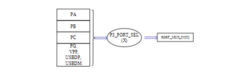 3、 gpio模拟输入,该输入信号可以作为长按复位(模拟)、边沿唤醒(模拟),通道0为 VBAT_DT/CHGFULL,通道 1为VBATCH,通道2为VPWRDT,长按复位可选择通道 1和通道2,即 VBATCH/VPWRDT, 边沿唤醒可选择通道 0~通道 2, 硬件设计上已固定, 唤醒参数中 wk_parm.aport[index],其中index并不与这里通道对应,接口映射到对应的硬件通道。
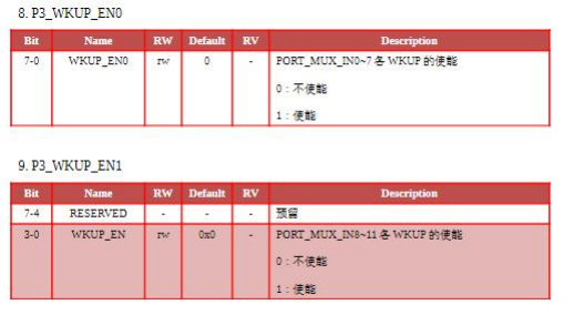
 4、 数字输入io通道选择/唤醒使能/长按复位(数字)控制/脉冲计数控制如下
AC701N All information provided in this document is subject to legal disclaimers © JL.V. 2019. All rights reserved.
User manual Rev1. 1——2022/5/30 6of27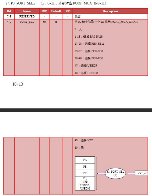 AC701N All information provided in this document is subject to legal disclaimers © JL.V. 2019. All rights reserved.
 AC701N All information provided in this document is subject to legal disclaimers © JL.V. 2019. All rights reserved.
 AC701N All information provided in this document is subject to legal disclaimers © JL.V. 2019. All rights reserved.
 4、 模拟输入io通道唤醒使能/长按复位控制(模拟)如下
 AC701N All information provided in this document is subject to legal disclaimers © JL.V. 2019. All rights reserved.
 AC701N All information provided in this document is subject to legal disclaimers © JL.V. 2019. All rights reserved.
Chapter 3 参数配置
3. 1 电源参数
//以下结构体只罗列需介绍部分 struct low_power_param {
u8 config; //低功耗使能,蓝牙&&系统空闲可进入低功耗
u8 osc_type; //低功耗晶振类型, btosc/lrc
u32 btosc_hz; //蓝牙晶振频率
//请配置vddiom>vddiow
u8 vddiom_lev; //vddiom
u8 vddiow_lev; //vddiow
u8 nkeep_vddio; //软关机状态下是否保持vddio 的电压,默认0保持
u32 osc_delay_us; //低功耗晶振起振延时,为预留配置。
u8 rtc_clk; //rtc时钟源,软关机根据此配置是否保持住相应时钟
u8 lpctmu_en; //低功耗触摸,软关机根据此配置是否保持住该模块
//以下两项可配置ram是否进入掉电模式
//参考memory mapping, ram 电源的控制变量如下
MEM_PWR_CPU_CON BIT(0)
MEM_PWR_RAM0_RAM3_CON BIT(1)
MEM_PWR_RAM4_RAM5_CON BIT(2)
MEM_PWR_RAM6_RAM7_CON BIT(3)
MEM_PWR_RAM8_RAM9_CON BIT(4)
MEM_PWR_PERIPH_CON BIT(5)
如配置为MEM_PWR_RAM8_RAM_CON,则表示为电源初始化/进入低功耗将RAM8/ RAM9,进入掉电的状态。
u8 mem_init_con; //初始化ram 电源
u8 mem_lowpower_con;//低功耗ram 电源
AC701N All information provided in this document is subject to legal disclaimers © JL.V. 2019. All rights reserved.
//pvdd 引脚是否外接dcdc,外接dcdc程序会将pvdd输出到PB8 引脚
u8 rvdd2pvdd;
//外挂flash gpio,使用外挂flash上下电接口及上电接口会操作改该引脚,默认将flash所有io 配置成高阻态,注意部分flash 的操作使用库接口会漏电,需要重写该函数。
void attribute ((weak)) hw_close_flash1(void);//外挂flash掉电接口
void attribute ((weak)) hw_flash1_pwr_en();//外挂flash上电接口
u8 lptmr_flow; //1:低功耗参数由用户配置 0:默认使用库参数
//由于sleep对时间节点较为严格,在低功耗流程请勿添加耗时操作,例如操作系统阻塞、软件延时、打印等
//若需要在低功耗流程(sleep callback、 deepsleep stash)添加相关操作,可调整低功耗时间t2(进入低功耗)、t4(出低功耗),单位为us,例如添加了一段程序在进sleep流程,耗时500us,则t2+500,若在出sleep流程增加耗时500us,则t4_lrc+500, t4_btosc+500。
| u32 t2; | //进sleep流程2 |
|---|---|
| u32 t4_lrc; | //出sleep流程2 lrc |
| u32 t4_btosc; | //出sleep流程2 osc |
| //以下参数为参考配置 |
powerdown:
t1: 1200, t2: 1700, t3_lrc: 750, t4_lrc: 3165, t3_btosc: 750, t4_btosc: 1665
poweroff:
t1: 1200, t2: 1700, t3_lrc: 1250, t4_lrc: 5050, t3_btosc: 1250, t4_btosc: 4050 u8 flash_pg;
};
3.2边沿唤醒参数
//最大同时支持gpio边沿唤醒12路,GPIOD、 GPIOE不支持唤醒#define MAX_WAKEUP_PORT 12
//最大同时支持模拟信号边沿唤醒3路,有LDOIN、 VBTCH、 CHARGE_FULL #define MAX_WAKEUP_ANA_PORT 3
AC701N All information provided in this document is subject to legal disclaimers © JL.V. 2019. All rights reserved.
struct port_wakeup {
u8 pullup_down_enable; //内部上下拉是否使能
| u8 edge; | //唤醒边沿条件 |
|---|---|
| u8 filter; | //滤波参数 gpio边沿唤醒滤波不可配制,默认滤波为128us |
| u8 iomap; | //唤醒gpio |
};
struct wakeup_param {
//io唤醒
const struct port_wakeup *port[MAX_WAKEUP_PORT];
//模拟信号唤醒
const struct port_wakeup *aport[MAX_WAKEUP_ANA_PORT];};
AC701N All information provided in this document is subject to legal disclaimers © JL.V. 2019. All rights reserved.
Chapter 4 唤醒
4. 1简介
PMU结构独立于系统,可以在系统睡眠或者软关机的情况下继续工作,提供多种唤醒功耗。
rtc、lvd(vddio低压)、 port edge(边沿唤醒)、 pcnt overflfow(计数溢出)支持唤醒低功耗状态,并产生P33 中断,所以边沿唤醒可以当作gpio外部中断使用,在睡眠状态唤醒可以产生中断,在软关机状态唤醒能记录到唤醒源。
LP_TMR、 LPCTMU、 LP VAD外设支持从睡眠状态下唤醒。
4.2 接口使用
头文件:include_lib/driver/cpu/$(CPU)/asm/ power/lp_wakeup. h
1、 边沿唤醒初始化,初始化之后默认使能
void power_wakeup_init(const struct wakeup_param *param)
2、gpio或模拟信号边沿唤醒使能/关闭,enable 为0则关闭,enable为1则使能。index表示通道号,对应唤醒参数中的数组号。gpio表示gpio号。
void power_wakeup_index_enable(u8 index, u8 enable);
void power_wakeup_gpio_enable(u8 gpio, u8 enable);
void power_awakeup_index_enable(u8 index, u8 enable);
void power_awakeup_gpio_enable(u8 gpio, u8 enable);
4、 gpio或模拟信号边沿类型设置, port表示gpio, edge表示边沿类型 void power_wakeup_gpio_edge(u8 gpio, POWER_WKUP_EDGE edge); void power_awakeup_gpio_edge(u8 gpio, POWER_WKUP_EDGE edge);
5、 配置gpio或模拟信号边沿唤醒回调,该接口只能被调用一次,会被覆盖。index为唤醒注册的通道,gpio为gpio号,edge表示边沿类型,因为模拟信号支持双边沿,所以回调函数包含了边沿信息。 void power_wakeup_set_callback(void ( *wakeup_callback)(u8 index, u8 gpio));
AC701N All information provided in this document is subject to legal disclaimers © JL.V. 2019. All rights reserved.
void power_awakeup_set_callback(void ( *wakeup_callback)(u8 index, u8 gpio, POWER_WKUP_EDGE edge));
6、 唤醒原因
//获取唤醒原因枚举如下 enum WAKEUP_REASON {
//WAKEUP
PWR_WK_REASON_PLUSE_CNT_OVERFLOW, //pcnt唤醒复位
PWR_WK_REASON_P11, //P11唤醒复位
PWR_WK_REASON_LPCTMU, //触摸唤醒复位
PWR_WK_REASON_PORT_EDGE, //数字io输入边沿唤醒复位
PWR_WK_REASON_ANA_EDGE, //模拟io输入边沿唤醒复位
PWR_WK_REASON_VDDIO_LVD, //vddio lvd唤醒复位
PWR_WK_REASON_EDGE_INDEX0, //p33 index0 io唤醒复位
PWR_WK_REASON_EDGE_INDEX1, //p33 index1 io唤醒复位
PWR_WK_REASON_EDGE_INDEX2, //p33 index2 io唤醒复位
PWR_WK_REASON_EDGE_INDEX3, //p33 index3 io唤醒复位
PWR_WK_REASON_EDGE_INDEX4, //p33 index4 io唤醒复位
PWR_WK_REASON_EDGE_INDEX5, //p33 index5 io唤醒复位
PWR_WK_REASON_EDGE_INDEX6, //p33 index6 io唤醒复位
PWR_WK_REASON_EDGE_INDEX7, //p33 index7 io唤醒复位
PWR_WK_REASON_EDGE_INDEX8, //p33 index8 io唤醒复位
PWR_WK_REASON_EDGE_INDEX9, //p33 index9 io唤醒复位
PWR_WK_REASON_EDGE_INDEX10, //p33 index10 io唤醒复位
PWR_WK_REASON_EDGE_INDEX11, //p33 index11 io唤醒复位
PWR_ANA_WK_REASON_FALLINIG_EDGE_LDOIN, //LDO5V上升沿唤醒复位
PWR_ANA_WK_REASON_RISING_EDGE_LDOIN, //LDO5V下降沿唤醒复位
PWR_ANA_WK_REASON_FALLING_EDGE_VBATCH, //VBATCH上升沿唤醒复位
PWR_ANA_WK_REASON_RISING_EDGE_VBATCH, //VBATCH下降沿唤醒复位};
//判断是否为index唤醒原因
AC701N All information provided in this document is subject to legal disclaimers © JL.V. 2019. All rights reserved.
u8 is_wakeup_source(enum WAKEUP_REASON index)
AC701N All information provided in this document is subject to legal disclaimers © JL.V. 2019. All rights reserved.
Chapter 5 复位
5. 1简介
系统复位的原因包括两种,第一种为系统复位源,第二种为自定义的复位源,例如断言软复位、异常软复位,是系统复位源的扩展,提供扩展信息、调试功能等。
5.2 接口使用
头文件:include_lib/driver/cpu/$(CPU)/asm/ power/power_reset. h
| //复位原因获取枚举如下 | |
|---|---|
| enum RST_REASON { | |
| / 主系统/ | |
| MSYS_P11_RST, | //P11复位 |
| MSYS_DVDD_POR_RST, | //DVDD上电 |
| MSYS_SOFT_RST, | //主系统软件复位 |
| MSYS_P2M_RST, | //低功耗唤醒复位(softoff advance && deepsleep) |
| MSYS_POWER_RETURN, | //主系统未被复位 |
| / * P11*/ | |
| P11_PVDD_POR_RST, | //pvdd上电 |
| P11_IVS_RST, | //低功耗唤醒复位(softoff legacy) |
| P11_P33_RST, | //p33复位 |
| P11_WDT_RST, | //看门狗复位 |
| P11_SOFT_RST, | //软件复位 |
| P11_MSYS_RST, | //主系统复位P11 |
| P11_POWER_RETURN, | //P11系统未被复位 |
| / * P33*/ | |
| P33 VDDIO POR RST, | //vddio上电复位(电池/vpwr供电) |
AC701N All information provided in this document is subject to legal disclaimers © JL.V. 2019. All rights reserved.
| P33_VDDIO_LVD_RST, | //vddio低压复位、上电复位(电池/vpwr供电) |
|---|---|
| P33_VCM_RST, | //vcm高电平短接复位 |
| P33_PPINR_RST, | //数字io输入长按复位 |
| P33_P11_RST, | //p 11系统复位p33, rset_mask=0 |
| P33_SOFT_RST, | //p33软件复位,一般软件复位指此系统复位源,所有系统会直接复位。 |
| P33_PPINR1_RST, | //模拟io输入长按复位,包括charge_full、 vatch、 ldoint、 vabt_det |
| P33_POWER_RETURN, | //p33系统未被复位。 |
| //SUB P33_EXCEPTION_SOFT_RST, | //异常软件复位 |
|---|---|
| P33_ASSERT_SOFT_RST, | //断言软件复位 |
};
//判断是否为index复位
u8 is_reset_source(enum RST_REASON index);
AC701N All information provided in this document is subject to legal disclaimers © JL.V. 2019. All rights reserved.
Chapter 6 校准
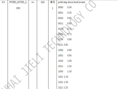
1、第一次上电部分电源会通过adc来校准,并写入vm。需要注意校准时环境,例如vddio接了串口,会有灌电流上电造成校准不对,档校准不对时重新擦除vm 即可校准。校准函数如下:
u8 wvdd_trim(u8 trim);
u8 pvdd_trim(u8 trim);
2、当发现此部分挡位与理论值相差大时可认为校准错误,一般校准错误程序跑不起来。以下挡位为 wvdd、 pvdd 的理论值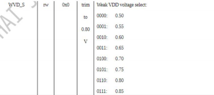
 AC701N All information provided in this document is subject to legal disclaimers © JL.V. 2019. All rights reserved.
Chapter 7 低功耗
7. 1 简介
低功耗模式包括softoff、powerdown、poweroff,以下描述从系统上来看,不包括pmu模块(p33 & p11)。 另外在该低功耗模式的基础上可保持部分模块,例如在powerdown模式下可保持晶振在运行。
softoff:所有模拟模块、数字模块都掉电。
powerdown:所有模拟模块掉电,数字模块低电、停止运行。
poweroff:所有模拟模块掉电,除rvdd外数字模块掉电、停止运行。
7.2 io配置
不漏电原则:数字输入die/dieh配置状态下,io为输入状态(cpu/外设/crossbar),外部没有确定电平有浮空漏电的危险,漏电电流不确定,请确保初始化外设/io 的状态,运行状态和低功耗模式通用。
sdk初始化:
1、 在port_init处理
2、 所有io die、 dieh关闭状态,上下拉关闭,过滤内置flash/ psram/ pinr/sdtap
外设/crossbar/cpu初始化:
根据不漏电原则配置io
sleep模式:
1、 在板级注册进入回调函数处理sleep_enter_callback、 sleep_exit_callback
2、 所有不使用的 io默认配置为高阻(输入模式、 上下拉关闭、数字输入关闭), 内置flash io 由 lib进行处理
3、 外设/crossbar 占用的io如果为输入状态,保持确定电平(确保外设初始化没问题就行)
4、 由于每个方案io使用情况不同,根据不漏电原则检查第2、 3点,代码如下:
AC701N All information provided in this document is subject to legal disclaimers © JL.V. 2019. All rights reserved.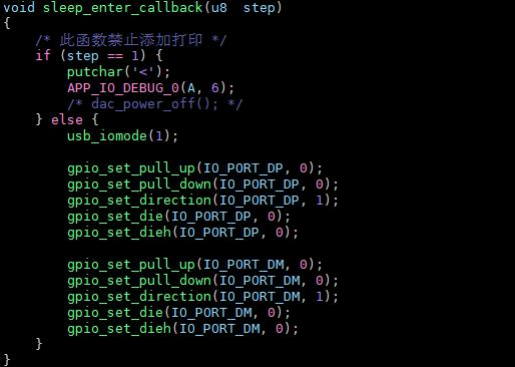 soffoff模式:
1、 在板级注册进入回调函数处理 board_set_soft_poweroff
2、 所有不使用的 io默认配置为高阻(输入模式、 上下拉关闭、数字输入关闭), 内置flash io 由 lib进行处理
3、 所有外设关闭,所有crossbar清除
4、由于每个io使用情况不同,根据不漏电原则检查第3点,soffoff模式根据使用外设需要保持部分io,代码如下
AC701N All information provided in this document is subject to legal disclaimers © JL.V. 2019. All rights reserved.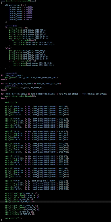 AC701N All information provided in this document is subject to legal disclaimers © JL.V. 2019. All rights reserved.
6.3 低功耗检查配置
在文件cpu/$(CPU)/ power_api.c。
1、 提供以下几个打印接口用于debug
void pmut_put_u8hex(u8 dat);
void pmu_put_u16hex(u16 dat);
void pmu_put_u32hex(u32 dat);
void pmu_put_u64hex(u64 dat);
void pmu_put_buf(const u8 *buf, int len);
2、 初始化 uart0 为 rc16m 时钟, 由于 rc16m 受温度及电压影响,请在 app_main 函数调用void config_p 11_baud()进行rc频率检测,源码如下:
AC701N All information provided in this document is subject to legal disclaimers © JL.V. 2019. All rights reserved.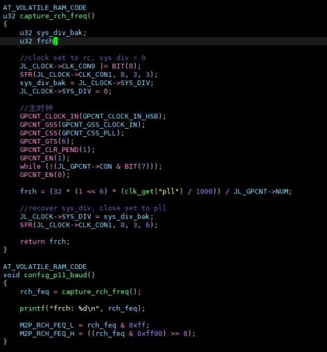 3、 由于需要使用rc16m打印,板级配置波特率如下:
#define TCFG_UART0_BAUDRATE 115200 //串口波特率配置
4、在对应debug点检查io/外设状态,初始化串口0,时钟源为rc16m,IO为PA05,波特率为115200,并且debug 点代码只能跑ram。
//powerdown/poweroff检查点 u8 sleep_safety_check(void)
//softoff检查点
u8 soff_safety_check(void)
//该函数会降所有io 的寄存器打印出来,包括方向、上下拉、数字输入控制位,检查对应的io状态
是否正确,源码如下 void check_gpio_safety()
AC701N All information provided in this document is subject to legal disclaimers © JL.V. 2019. All rights reserved.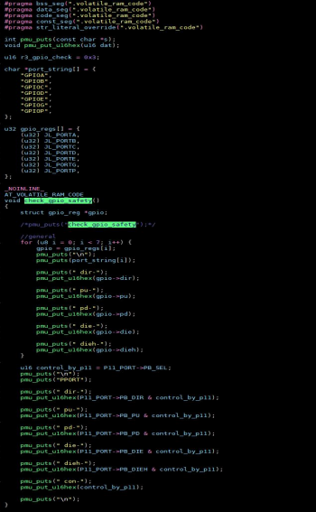 AC701N All information provided in this document is subject to legal disclaimers © JL.V. 2019. All rights reserved.
Chapter 8 客户常见问题反馈解答
Q1:
Q2:
AC701N All information provided in this document is subject to legal disclaimers © JL.V. 2019. All rights reserved.